Came across a series of videos explaining the intracacies of modern silicon chip fabricaion (Fab) , and was fascinated by the sheer complexity of making tiny transistors and circuits. In the heart of the silicon revolution, where chips smaller than snowflakes power our world, lies a Dutch titan: ASML. Their claim to fame? Lithography machines, marvels of engineering that etch the intricate circuitry of modern microchips with mind-boggling precision. But ASML’s story isn’t just about miniaturization; it’s about a relentless pursuit of the ever-smaller, the ever-faster, and the ever-more-powerful.
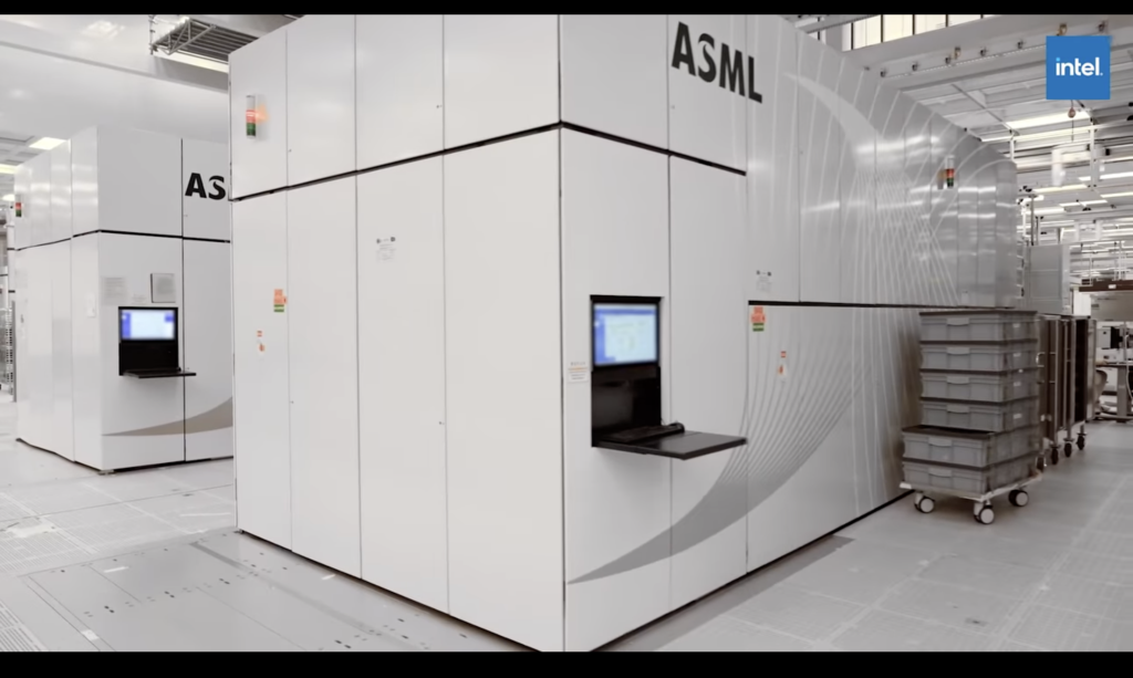
ASML deep ultraviolet (DUV) lithography system
Imagine a light so intense, it can carve patterns on a silicon wafer a million times thinner than a human hair. That’s the magic of ASML’s deep ultraviolet (DUV) lithography systems. Using cutting-edge optics and lasers, these machines project microscopic blueprints onto the wafer, layer by layer, building the intricate landscapes of transistors and interconnects that form the lifeblood of modern chips.
ASML extreme ultraviolet (EUV) lithography system
But DUV is just the first act. To keep pace with Moore’s Law, the relentless miniaturization of chips, ASML has ventured into the realm of the extreme: extreme ultraviolet (EUV) lithography. Here, the light used to etch the circuits has a wavelength shorter than the width of a single atom! This allows for even tinier features, pushing the boundaries of what’s possible.
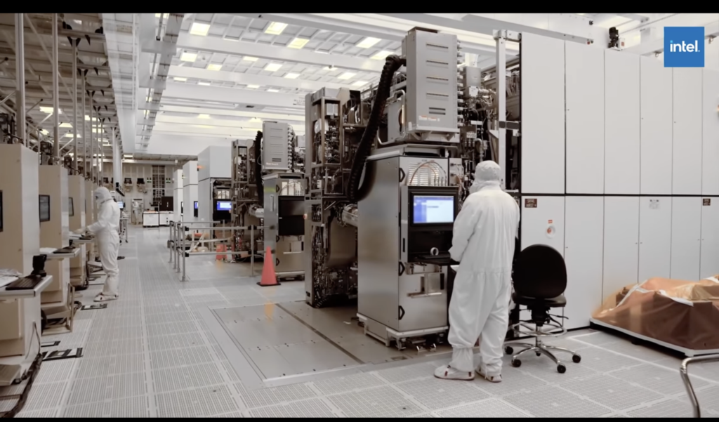
The innovations don’t stop at light. ASML’s machines are marvels of precision engineering. Imagine a robotic arm moving a multi-ton wafer with the accuracy of a brain surgeon, all while maintaining a vacuum environment cleaner than the Antarctic desert. These machines are testaments to human ingenuity, pushing the limits of physics and mechanics.
Here’s a short video explaining the process…
If you want a more deep dive into all things Microchip fabrication, check out an excellent YouTube Channel -Asianometry .
The future of ASML is as bright as the lasers in their machines. They’re constantly exploring new technologies, like high-numerical-aperture (NA) EUV and next-generation immersion techniques, to keep miniaturization on track. With each breakthrough, they shrink the impossible, paving the way for even more powerful and efficient chips that will shape the world of tomorrow. www.wired.com
So, the next time you hold a smartphone in your hand, take a moment to appreciate the invisible wonders within. Remember the Dutch giants at ASML, whose relentless pursuit of the ever-smaller has brought us to the cutting edge of the silicon revolution.